NOR ROM
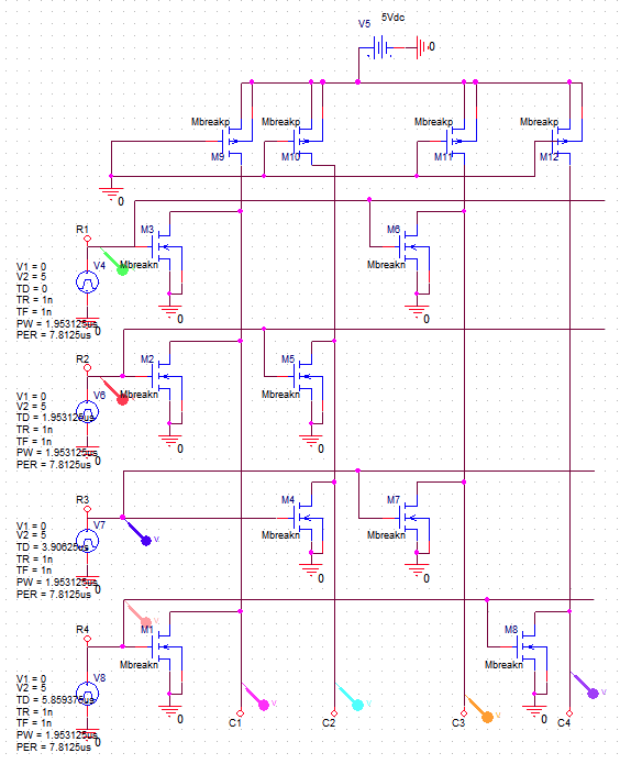
Read-Only Memory (ROM) is a combinational circuit that outputs a specific pattern for each memory address. These addresses are the inputs to the circuit. The output for each memory address is based on the transistor orientation designed in that memory line. A simple implementation of the ROM circuit is called the NOR ROM implementation. This implementation involves pseudo-PMOS logic. This implementation makes resizing the NMOS transistors in the circuit very important to get accurate results. For a 2^n input memory, there usually is an n to 2n decoder circuit attached to the ROM array. For testing a 4X4 ROM circuit, the decoder circuit can be replaced by an 4-bit shift register.
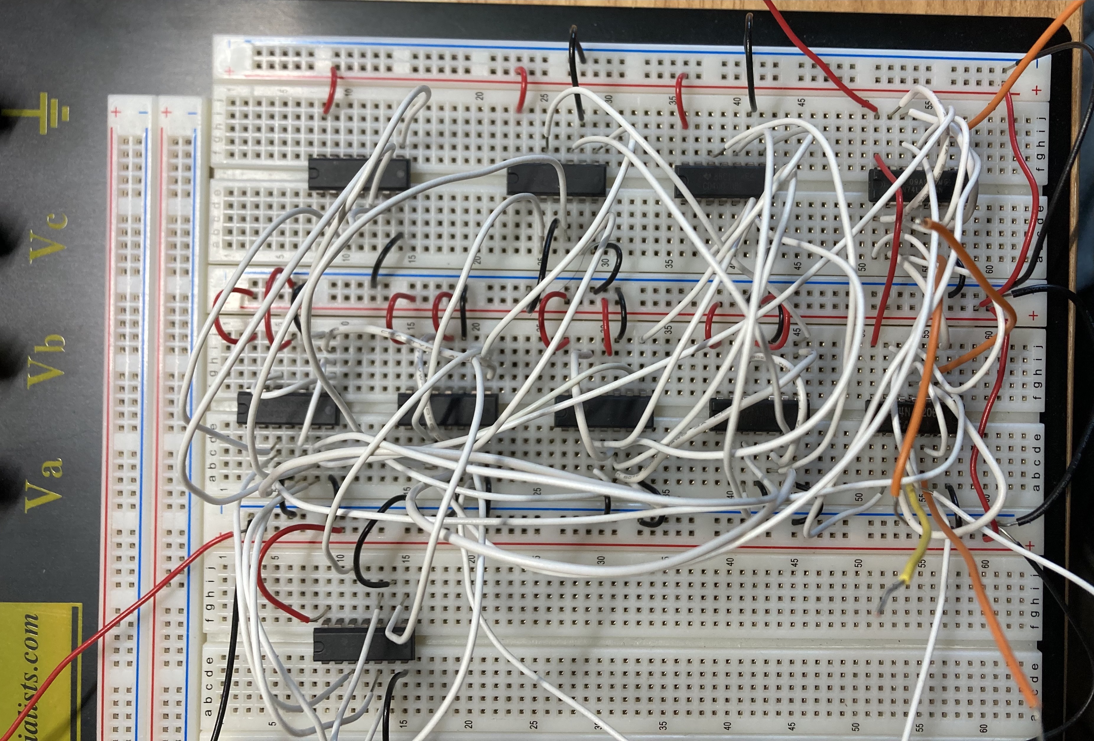
Fig. 1: 4x4 NOR-ROM Memory Breadboard Implementation

Fig. 2: 4x4 NOR-ROM Memory PSPICE Schematic

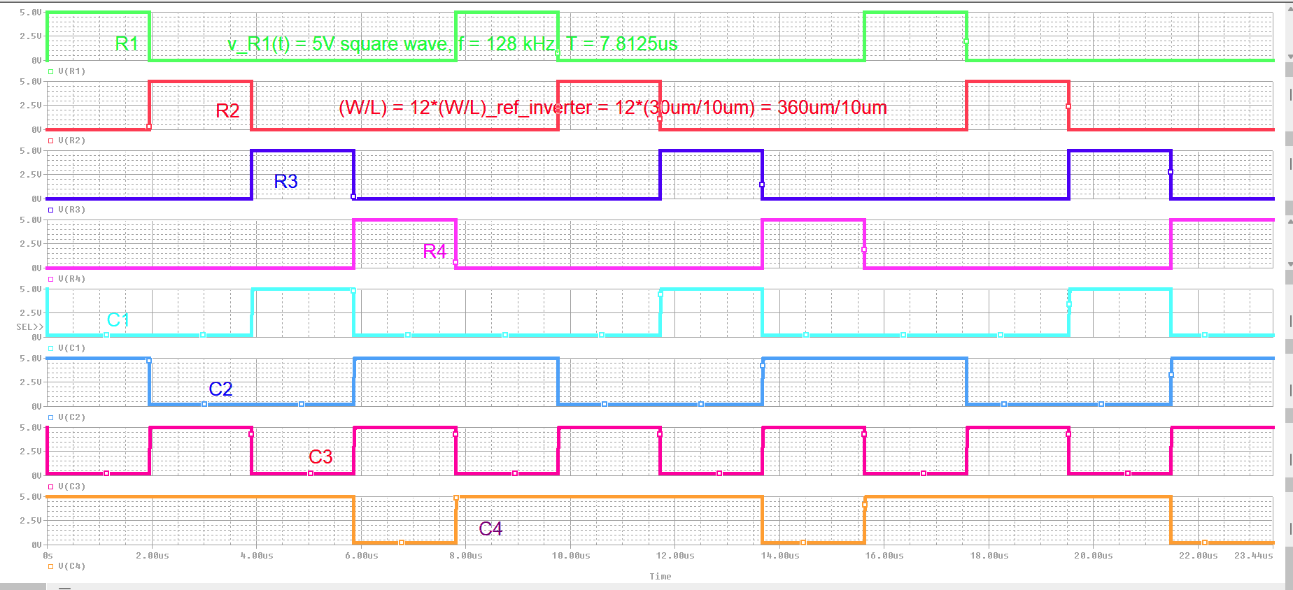
Fig. 3: 4x4 NOR-ROM PSPICE Simulation
